New Technique Protects Fragile Quantum Materials Without Complex Stacking
A simple electron-beam evaporation method shields delicate two-dimensional quantum crystals from environmental degradation while enabling clean device fabrication.
The rapid advancement of two-dimensional materials has unlocked exciting possibilities for nanoelectronics, photonics, and quantum information processing. However, a persistent bottleneck in the field is the vulnerability of these atomically thin crystals to environmental degradation, fabrication-induced disorder, and surface defects. Many high-performance materials begin to degrade immediately upon exposure to ambient air, oxidizing or reacting with the photoresists and solvents required during standard cleanroom device fabrication. To combat this vulnerability, researchers have heavily relied on encapsulating flakes within hexagonal boron nitride. While effective at preserving pristine surfaces, hexagonal boron nitride encapsulation is notoriously difficult to scale, limited to thin stacks, and requires tedious manual alignment and specialized transfer techniques.
Furthermore, standard encapsulation usually demands that devices be patterned prior to sealing, meaning any subsequent etching steps to open electrical contact windows risk damaging the underlying quantum material. Alternative oxide deposition techniques, such as atomic layer deposition, often rely on reactive precursors or moisture exposure that can ruin fragile low-dimensional samples. Addressing these longstanding manufacturing hurdles, a multi-institutional research team has detailed a simpler, scalable alternative, published in Nano Letters, demonstrating that room-temperature electron-beam evaporated aluminum oxide effectively bridges the gap between material protection and straightforward device manufacturing.
Protecting Air-Sensitive Metals and Superconductors
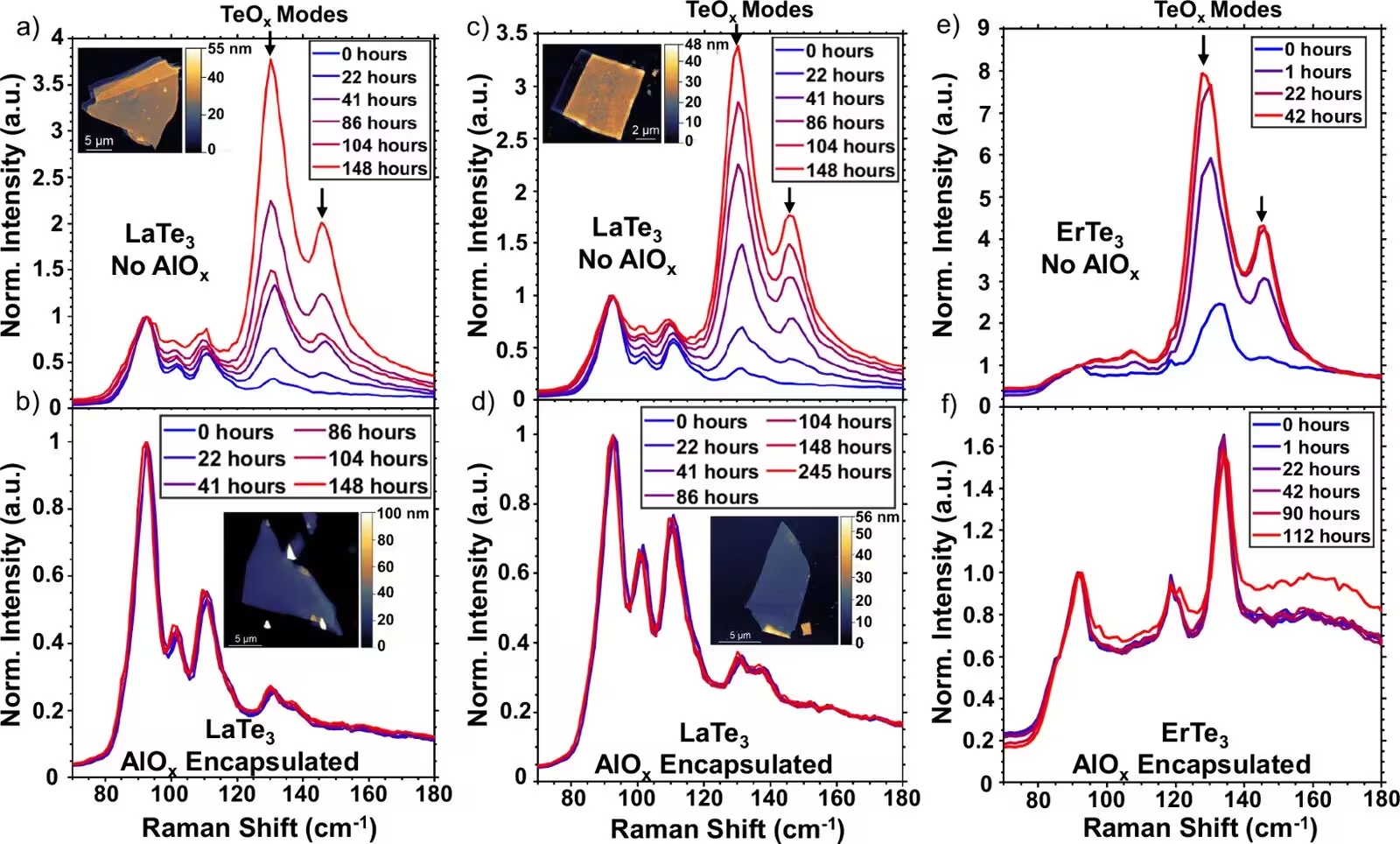
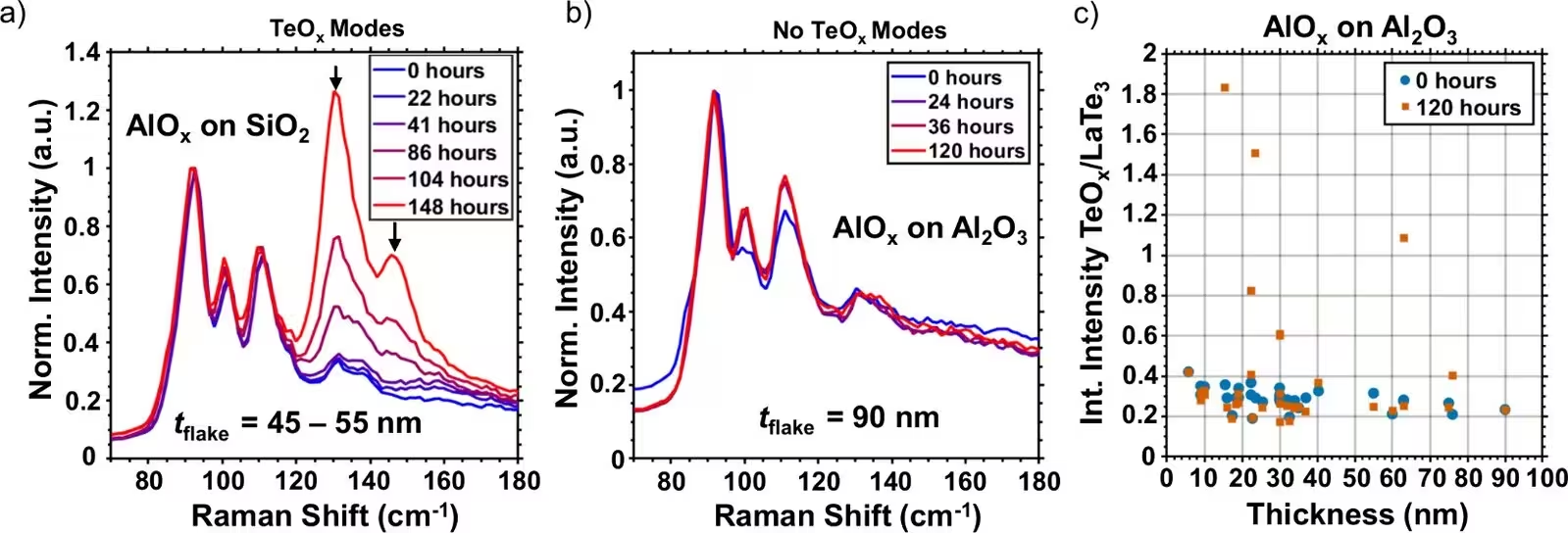
The research team evaluated their encapsulation strategy across three diverse classes of low-dimensional systems known for their delicate physics and extreme sensitivity to air. The first material family investigated was the rare-earth tritellurides, which are high-mobility quasi-two-dimensional metals that host exotic charge-density-wave phases. Despite their fascinating electronic properties, these materials are highly susceptible to tellurium oxide formation, which ruins unshielded flakes within hours of ambient exposure. By depositing an aluminum oxide layer via electron-beam evaporation, the team successfully suppressed oxidation, allowing the rare-earth tritelluride flakes to maintain their pristine Raman spectra and smooth surface topographies over extended periods.
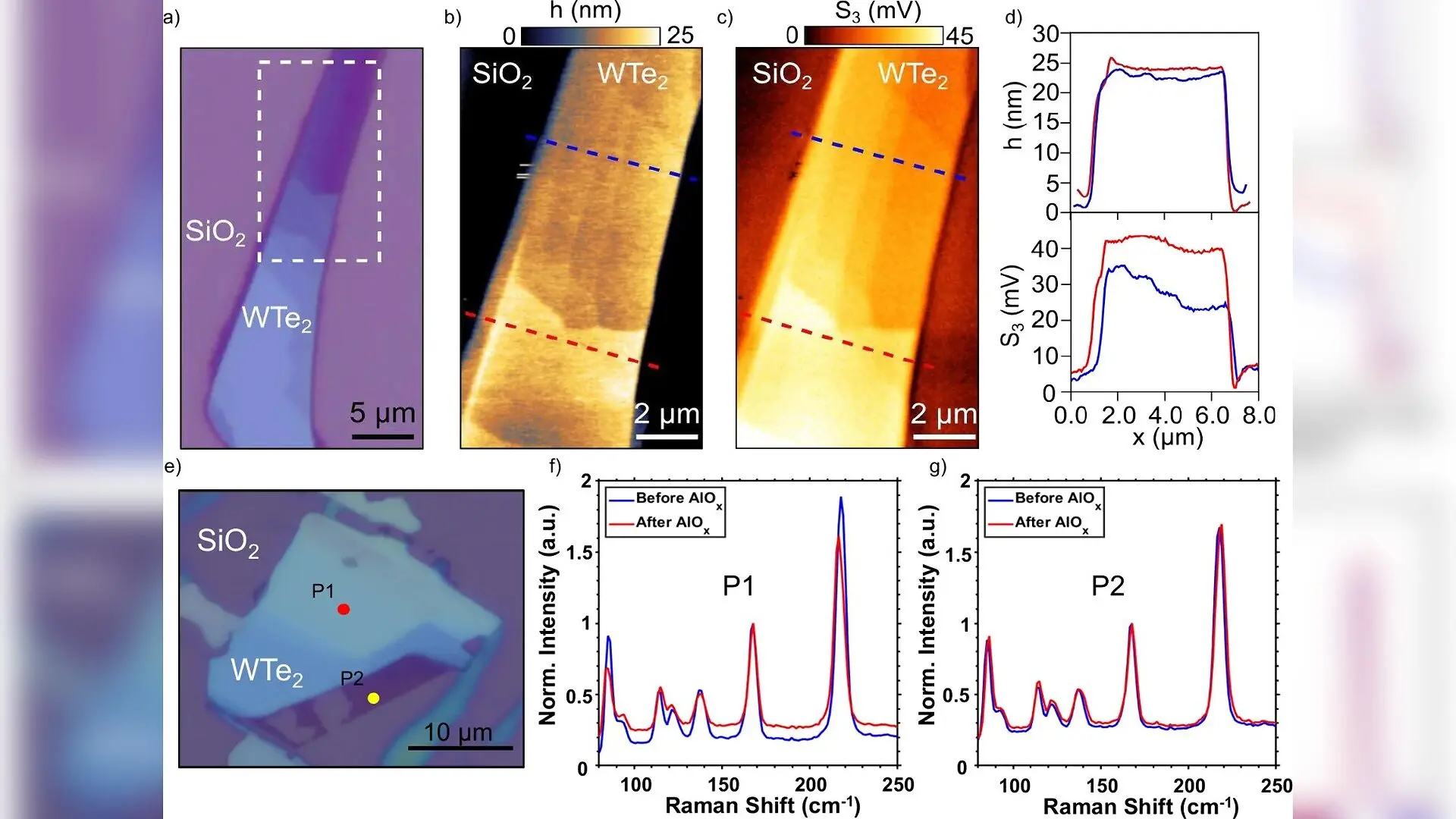
The researchers also targeted semimetallic transition metal ditellurides, which exhibit rich thickness-dependent optical behavior and plasmonic properties. Traditional thick capping layers can severely attenuate near-field optical signals, creating a frustrating trade-off between environmental protection and optical accessibility. By applying an ultrathin three-nanometer aluminum oxide coating, the team protected the delicate flakes while preserving their near-field optical response, allowing single-layer variations to remain clearly distinguishable during advanced nanoscale imaging.
Finally, the team examined iron-based superconducting crystals, whose delicate superconducting transition temperatures and transport properties are easily disrupted by chemical processing or air exposure. By utilizing the thin aluminum oxide layer not just as a permanent cap, but as a clever sacrificial fabrication mask, the researchers were able to pattern electrical contacts directly through the protective coating without exposing the underlying crystal to harmful photoresists or solvents.
A Scalable Path for Quantum Device Integration
The success of this sacrificial mask approach relies on a neat chemical compatibility trick. During standard cleanroom development, the exposed portions of the thin aluminum oxide mask dissolve rapidly in tetramethylammonium hydroxide-based developers, cleanly opening contact windows without requiring aggressive dry etching steps. Once the fabrication workflow is complete, the entire device can be further sealed with a thicker aluminum oxide cap if long-term environmental isolation is desired.
Transport measurements performed on the fabricated superconductor devices confirmed that metallic normal-state behavior and sharp transitions to zero-resistance states were fully preserved, regardless of whether the devices were processed through the sacrificial mask or encapsulated afterward. Quantitative analysis of the transition widths even revealed improved device quality when using the sacrificial protection strategy compared to conventional unprotected processing routes.
By bypassing the need for complex transfer equipment, polymer stamp assemblies, and alignment steps required by alternative stacking methods, this electron-beam evaporation strategy integrates smoothly with standard cleanroom lithography. The findings provide a versatile, scalable toolkit for materials scientists, paving the way for the reliable fabrication and study of fragile quantum materials in future electronic and photonic architectures.
The research was published in Nano letters on October 14, 2026.
This article has been fact checked for accuracy, with information verified against reputable sources. Learn more about us and our editorial process.
Last reviewed on .
Article history
- Latest version
Reference(s)
- Natale, Gabriel., et al. “Scalable, Simple, and Versatile Encapsulation of 2D Materials and Devices.” Nano Letters, vol. 26, no. 40, October 3, 2026, pp. 13904-13912. American Chemical Society (ACS), doi: 10.1021/acs.nanolett.6c03297. <https://doi.org/10.1021/acs.nanolett.6c03297>.
Cite this page:
- Posted by John Williams