Quantum Puddles Reveal Hidden Glassy Dynamics in Layered Materials
Advanced optical and Raman measurements expose how local charge-density-wave puddles synchronize to drive macroscopic transitions in quantum crystals.
Quantum materials often defy simple descriptions because their internal electronic phases are governed by nanoscale spatial inhomogeneity. Instead of uniform states spanning a crystal, these systems frequently form localized patches or puddles where distinct forms of electronic order take hold. A prominent manifestation of this phenomenon appears in materials hosting incommensurate charge-density-waves, where the underlying periodic modulation of charge density breaks into locally commensurate domains. Understanding how these domains interact and synchronize remains one of the central challenges in condensed matter physics.
To explore this complex behavior, an international team of researchers focused on 2H-NbSe2, a layered transition metal dichalcogenide where superconductivity and unconventional charge-density-wave phases coexist at low temperatures. Because its simpler chemical structure helps isolate competing interactions, 2H-NbSe2 serves as an ideal testbed for investigating how local puddle dynamics influence macroscopic material properties. The research findings were published in Nano Letters, offering a detailed look at the hidden collective behavior of these quantum states.
Probing Lattice and Charge Interactions
The investigators combined temperature-dependent Raman scattering with ultrafast optical pump-probe spectroscopy on bulk-like mechanically exfoliated flakes of 2H-NbSe2. Through Raman susceptibility measurements, they observed that the charge-density-wave amplitude mode exhibits an asymmetric Fano line shape. This distinctive profile indicates a strong quantum mechanical interference, or coupling, between the crystal lattice’s interlayer shear vibrations and the electronic charge-density-wave amplitude mode.
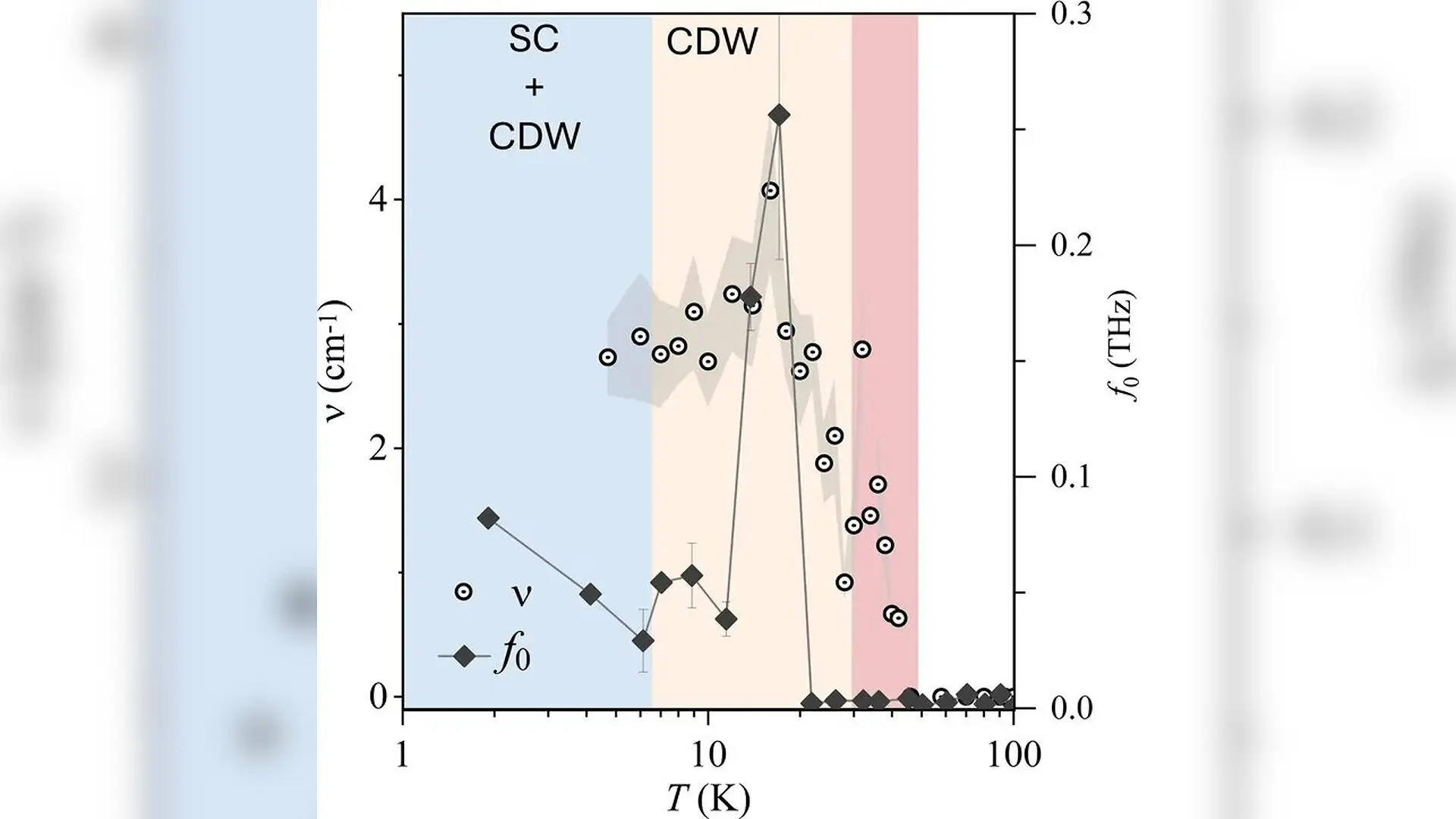
While previous studies noted the existence of charge-density-wave domains spanning roughly ten nanometers, tracking their temporal evolution under varying temperatures proved challenging. By employing ultrafast time-resolved reflectivity, the research team detected a low-frequency coherent overdamped oscillation that sets in precisely around 17 Kelvin, well within the charge-density-wave regime which has a transition temperature near 28 Kelvin. This oscillation operates at approximately 0.2 terahertz, making it significantly slower than the primary charge-density-wave amplitude mode found near 1.2 terahertz.
Unveiling Glassy Collective Dynamics
Further analysis of the temperature-dependent reflectivity data revealed that the electron relaxation time diverges significantly as the crystal cools through the 17 Kelvin mark. This divergence points directly to a critical slowing down of electronic and lattice degrees of freedom, signaling the onset of glassy dynamics driven by the collective movement of charge-density-wave puddles. The researchers attribute this glassy behavior to electronic frustration arising from fierce competition between different charge-density-wave commensuration orders.
Intriguingly, as the temperature drops further below 14 Kelvin, the oscillation frequency undergoes a softening before increasing monotonically as the system approaches its superconducting transition temperature near 7 Kelvin. This dual behavior suggests that early superconducting fluctuations begin to impact the underlying charge-density-wave order and its associated puddle dynamics before zero resistance is fully achieved.
Implications for Quantum Material Design
The convergence of Raman scattering data and ultrafast optical measurements provides a coherent picture of how microscopic inhomogeneities dictate macroscopic phenomena. The emergence of Fano coupling explains why high-frequency charge-density-wave oscillations were previously difficult to isolate in ultrafast experiments, while also highlighting how interlayer shear strain suppresses overall phase coherence.
These insights bridge long-standing gaps regarding the microscopic origins of charge-density-waves and preformed electronic order in layered crystals. By demonstrating how local puddle dynamics shape the global response of a quantum material, the work establishes a conceptual framework that could guide the future engineering of advanced van der Waals devices and superconducting heterostructures.
The research was published in Nano letters on October 21, 2026.
This article has been fact checked for accuracy, with information verified against reputable sources. Learn more about us and our editorial process.
Last reviewed on .
Article history
- Latest version
Reference(s)
- Kumbhakar, Shreya., et al. “Dynamics of Charge-Density-Wave Puddles in 2 H -NbSe2.” Nano Letters, vol. 26, no. 41, October 12, 2026, pp. 14376-14383. American Chemical Society (ACS), doi: 10.1021/acs.nanolett.6c03967. <https://doi.org/10.1021/acs.nanolett.6c03967>.
Cite this page:
- Posted by John Williams